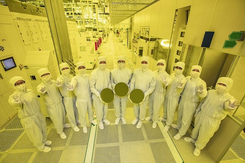
Samsung marks its first shipment of cutting-edge 3nm chips
 |
The chips apply Gate-All-Around (GAA) technology. The second-generation 3nm process helps reduce power consumption by up to 50 per cent, improve performance by 30 per cent, and reduce the required area by 35 per cent in comparison with the existing process.
Samsung has surpassed its rival TSMC of Taiwan in the race to advance its chipmaking technology. As a result, Samsung is expected to secure more orders from customers who are seeking powerful chips that enable smaller, faster, and more efficient technology products, as reported by newswire Yonhap.
According to Yonhap, TSMC will begin mass production of 3nm chips in the second half of the year. Samsung and TSMC have been in fierce competition by bringing the most advanced and efficient chips to the mass market.
"Samsung opened a new chapter in the foundry business today, with the start of mass production of 3nm chips," Kyung Kye-hyun, CEO of Samsung's device solutions division, which supervises the chip business, said at the ceremony at its Hwaseong production lines.
"The development of the GAA technology earlier than expected as an alternative to the previous process was an innovative breakthrough," Kyung added.
Samsung claimed that it began developing the GAA technology in the early 2000s and was successful in implementing it on the 3nm node in 2017.
High-performance computing is the first use case of the 3nm GAA technology. Samsung plans to expand the application into other product categories.
Since the third quarter of 2021, Samsung Electronics has been providing proven design infrastructure through extensive preparation with Samsung Advanced Foundry Ecosystem partners including Ansys, Cadence, Siemens, and Synopsys, to help customers perfect their products in a reduced period of time.
What the stars mean:
★ Poor ★ ★ Promising ★★★ Good ★★★★ Very good ★★★★★ Exceptional
Related Contents
Latest News
More News
- Posco Future M’s $282 million investment set for Q3 (April 25, 2026 | 09:00)
- $2.3 billion Quynh Lap LNG plant to kick off in May (April 24, 2026 | 17:26)
- Hyosung targets high-voltage equipment investment in Vietnam (April 24, 2026 | 17:21)
- Japanese food giant chooses Vietnam for ready-mix flour production (April 24, 2026 | 16:37)
- Vietnam nears investment grade as reforms and growth strengthen outlook (April 24, 2026 | 15:02)
- AI and semiconductors drive new wave of Vietnam-South Korea business ties (April 24, 2026 | 14:57)
- Vietnam and South Korea to deepen ties on industry, investment, technology (April 24, 2026 | 12:33)
- Long Son Petrochemicals to suspend operations from mid-May (April 24, 2026 | 12:24)
- SK Group to foster AI ecosystem development in Vietnam (April 24, 2026 | 12:22)
- South Korea and Vietnam deepen strategic agricultural partnership (April 23, 2026 | 17:21)

 Tag:
Tag:


 Mobile Version